Note
Hello, welcome to the SunFounder Raspberry Pi & Arduino & ESP32 Enthusiasts Community on Facebook! Dive deeper into Raspberry Pi, Arduino, and ESP32 with fellow enthusiasts.
Why Join?
Expert Support: Solve post-sale issues and technical challenges with help from our community and team.
Learn & Share: Exchange tips and tutorials to enhance your skills.
Exclusive Previews: Get early access to new product announcements and sneak peeks.
Special Discounts: Enjoy exclusive discounts on our newest products.
Festive Promotions and Giveaways: Take part in giveaways and holiday promotions.
👉 Ready to explore and create with us? Click [here] and join today!
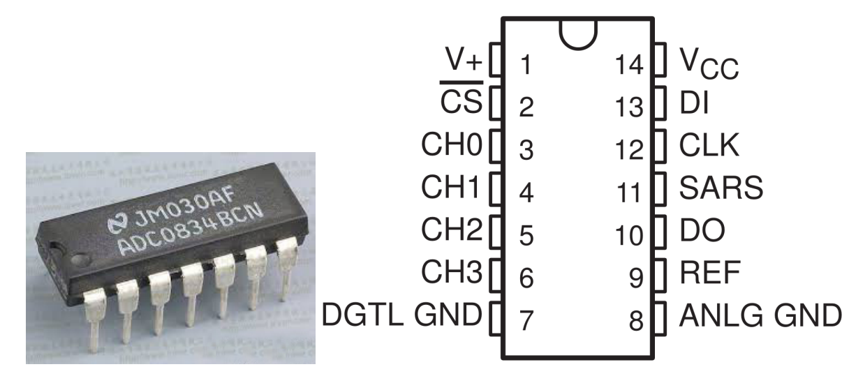
ADC0834
ADC0834 is an 8-bit successive approximation analog-to-digital converter that is equipped with an input-configurable multichannel multi-plexer and serial input/output. The serial input/output is configured to interface with standard shift registers or microprocessors.
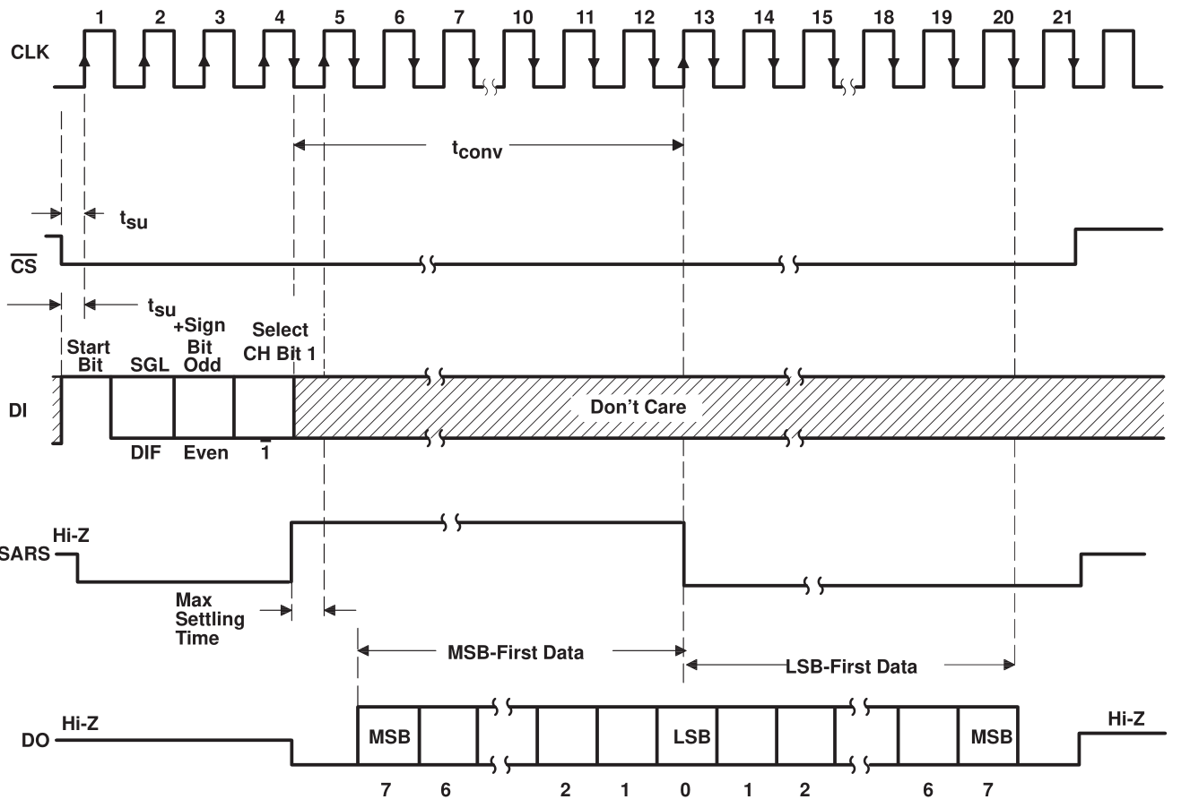
Sequence of Operation
A conversion is initiated by setting CS low, which enables all logic circuits. CS must be held low for the complete conversion process. A clock input is then received from the processor. On each low-to-high transition of the clock input, the data on DI is clocked into the multiplexer address shift register. The first logic high on the input is the start bit. A 3- to 4-bit assignment word follows the start bit. On each successive low-to-high transition of the clock input, the start bit and assignment word are shifted through the shift register. When the start bit is shifted into the start location of the multiplexer register, the input channel is selected and conversion starts. The SAR Statu output (SARS) goes high to indicate that a conversion is in progress, and DI to the multiplexer shift register is disabled the duration of the conversion.
An interval of one clock period is automatically inserted to allow the selected multiplexed channel to settle. The data output DO comes out of the high-impedance state and provides a leading low for this one clock period of multiplexer settling time. The SAR comparator compares successive outputs from the resistive ladder with the incoming analog signal. The comparator output indicates whether the analog input is greater than or less than the resistive ladder output. As the conversion proceeds, conversion data is simultaneously output from the DO output pin, with the most significant bit (MSB) first.
After eight clock periods, the conversion is complete and the SARS output goes low. Finally outputs the least-significant-bit-first data after the MSB-first data stream.
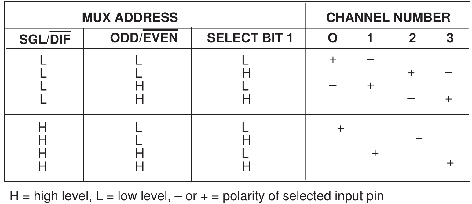
ADC0834 MUX ADDRESS CONTROL LOGIC TABLE
Example
2.1.7 Potentiometer (C Project)
2.2.1 Photoresistor (C Project)
2.2.2 Thermistor (C Project)
3.1.4 Smart Fan (C Project)
3.1.5 Battery Indicator (C Project)
3.1.7 Overheat Monitor (C Project)
2.1.7 Potentiometer (Python Project)
2.2.1 Photoresistor (Pyhton Project)
2.2.2 Thermistor (Pyhton Project)
4.1.10 Smart Fan (Pyhton Project)
4.1.11 Battery Indicator (Pyhton Project)
4.1.13 Overheat Monitor (Pyhton Project)