Note
Hello, welcome to the SunFounder Raspberry Pi & Arduino & ESP32 Enthusiasts Community on Facebook! Dive deeper into Raspberry Pi, Arduino, and ESP32 with fellow enthusiasts.
Why Join?
Expert Support: Solve post-sale issues and technical challenges with help from our community and team.
Learn & Share: Exchange tips and tutorials to enhance your skills.
Exclusive Previews: Get early access to new product announcements and sneak peeks.
Special Discounts: Enjoy exclusive discounts on our newest products.
Festive Promotions and Giveaways: Take part in giveaways and holiday promotions.
👉 Ready to explore and create with us? Click [here] and join today!
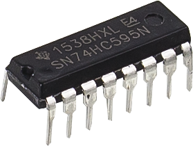
74HC595
The 74HC595 consists of an 8−bit shift register and a storage register with three−state parallel outputs. It converts serial input into parallel output so you can save IO ports of an MCU. When MR (pin10) is high level and OE (pin13) is low level, data is input in the rising edge of SHcp and goes to the memory register through the rising edge of SHcp. If the two clocks are connected together, the shift register is always one pulse earlier than the memory register. There is a serial shift input pin (Ds), a serial output pin (Q) and an asynchronous reset button (low level) in the memory register. The memory register outputs a Bus with a parallel 8-bit and in three states. When OE is enabled (low level), the data in memory register is output to the bus.
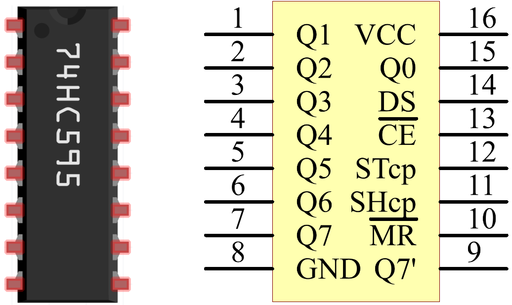
Pins of 74HC595 and their functions:
Q0-Q7: 8-bit parallel data output pins, able to control 8 LEDs or 8 pins of 7-segment display directly.
Q7’: Series output pin, connected to DS of another 74HC595 to connect multiple 74HC595s in series
MR: Reset pin, active at low level;
SHcp: Time sequence input of shift register. On the rising edge, the data in shift register moves successively one bit, i.e. data in Q1 moves to Q2, and so forth. While on the falling edge, the data in shift register remain unchanged.
STcp: Time sequence input of storage register. On the rising edge, data in the shift register moves into memory register.
CE: Output enable pin, active at low level.
DS: Serial data input pin
VCC: Positive supply voltage.
GND: Ground.
Example
1.1.4 7-segment Display (C Project)
1.1.5 4-Digit 7-Segment Display (C Project)
3.1.1 Counting Device (C Project)
3.1.6 Traffic Light (C Project)
3.1.12 GAME - 10 Second (C Project)
1.1.4 7-segment Display (Python Project)
1.1.5 4-Digit 7-Segment Display (Python Project)
4.1.7 Counting Device (Pyhton Project)
4.1.12 Traffic Light (Python Project)
4.1.18 GAME - 10 Second (Pyhton Project)