74HC595
Do you ever find yourself wanting to control a lot of LEDs, or just need more I/O pins to control buttons, sensors, and servos all at once? Well, you can connect a few sensors to Arduino pins, but you will soon start to run out of pins on the Arduino.
The solution is to use “shift registers”. Shift registers allow you to expand the number of I/O pins you can use from the Arduino (or any microcontroller). The 74HC595 shift register is one of the most famous.
The 74HC595 basically controls eight independent output pins and uses only three input pins. If you need more than eight additional I/O lines, you can easily cascade any number of shift registers and create a large number of I/O lines. All this is done by so-called shifting.
Features
8-Bit serial-in, parallel-out shift
Wide operating voltage range of 2 V to 6 V
High-current 3-state outputs can drive up to 15LSTTL loads
Low power consumption, 80-µA max ICC
Typical tPD = 14 ns
±6-mA output drive at 5 V
Low input current of 1 µA max
Shift register has direct clear
Pins of 74HC595 and their functions:
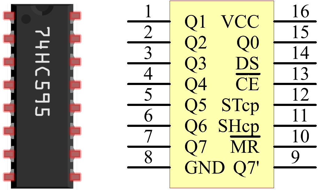
Q0-Q7: 8-bit parallel data output pins, able to control 8 LEDs or 8 pins of 7-segment display directly.
Q7’: Series output pin, connected to DS of another 74HC595 to connect multiple 74HC595s in series
MR: Reset pin, active at low level;
SHcp: Time sequence input of shift register. On the rising edge, the data in shift register moves successively one bit, i.e. data in Q1 moves to Q2, and so forth. While on the falling edge, the data in shift register remain unchanged.
STcp: Time sequence input of storage register. On the rising edge, data in the shift register moves into memory register.
CE: Output enable pin, active at low level.
DS: Serial data input pin
VCC: Positive supply voltage.
GND: Ground.
Functional Diagram
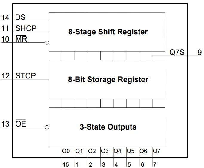
Working Principle
When MR (pin10) is high level and OE (pin13) is low level, data is input in the rising edge of SHcp and goes to the memory register through the rising edge of STcp.
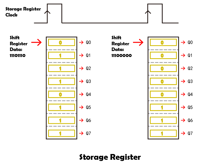
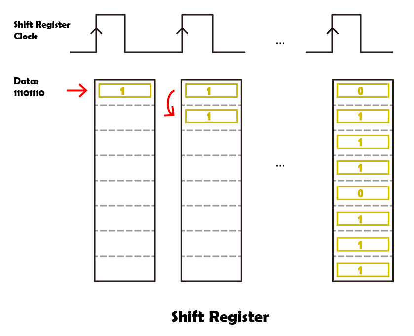
Shift Register
Suppose, we want to input the binary data 1110 1110 into the shift register of the 74hc595.
The data is input from bit 0 of the shift register.
Whenever the shift register clock is a rising edge, the bits in the shift register are shifted one step. For example, bit 7 accepts the previous value in bit 6, bit 6 gets the value of bit 5, etc.
Storage Register
When the storage register is in the rising edge state, the data of the shift register will be transferred to the storage register.
The storage register is directly connected to the 8 output pins, Q0 ~ Q7 will be able to receive a byte of data.
The so-called storage register means that the data can exist in this register and will not disappear with one output.
The data will remain valid and unchanged as long as the 74HC595 is powered on continuously.
When new data comes, the data in the storage register will be overwritten and updated.